
(originally published by byuu on: 2020-01-21)
SNES emulation has come a long way from its inception in the 1990s.
These days, I am able to keep my bug tracker free of game-related issues approximately 95% of the time, and new issues are usually very minor and quickly resolved.
We are in a good place with our emulation of nearly all SNES components, with the sole exception of the SNES PPUs, or video processors. When it comes to scanline timing, we have more than perfected that, but when it comes to the individual pixel timings, needed for raster effect accuracy, it is the one weak area left in SNES emulation.
In practice, I can only name one game (Air Strike Patrol) that intentionally relied on SNES raster (mid-scanline) effects, so the importance of this is easy to downplay, however for the sake of completion it represents the final frontier of SNES emulation research.
When I first entered the SNES emulation scene in 2004, things were in bad shape: aside from high-level emulation of SNES coprocessors, no substantial core progress had been made since around 1999 or so.
Emulators back then worked on a principle I like to call whack-a-mole emulation: whenever a game wasn’t functioning, a fix would be devised that would seemingly make that specific game work, but the fixes weren’t being verified as accurate to real hardware. Over time, the fixes would turn out to be wrong and break other games. Fixes for those games would break yet more games. And then fixes for those would break the original game that started this cycle. Rinse, repeat.
The thing I knew we needed from day one was to not prioritize fixing specific games, but rather to understand how the actual hardware operated, and to implement correct, hardware-verified fixes.
The key insight that made this possible was me devising library code that could seek to exact cycle positions within each emulated video frame, execute code of my choosing, and then analyze the results. By making loops over ranges of cycle positions, it became possible to analyze and determine exactly where various operations on the SNES occurred.
This worked amazingly well, and combined with the help of others over the next fifteen years, we were able to basically perfect the internal operations of the CPU (central processor) and SMP (audio processor) inside the SNES.
Sometime later, a developer by the name of blargg appeared to tackle the SNES DSP (audio generator), by taking advantage of cycle-timed SMP code and a key feature of the DSP: the echo buffer. The DSP would write all generated audio samples into this echo buffer, and from here it was possible to analyze the results of audio mixing, allowing us to once again reverse engineer and perfectly emulate every internal operation of the SNES DSP.
After a successful coprocessor decapping project, I was able to emulate all of the SNES coprocessors using low-level emulation.
And finally, to cap things off, several important new hardware test ROMs and a lot of hard work enabled me to emulate cycle-level timings of the SuperFX CPU’s instruction and pixel caches, and bus-conflict arbitration stall timings of the SA-1 CPU.
Thousands of additional hours into other coprocessors (decompressors, real-time clocks, memory mappers, etc) has led to a state of near-perfect SNES emulation.
That is, with the one exception of the SNES PPUs.
To generate video, the SNES relies on two PPU (picture processing unit) chips, the PPU1 and PPU2.
Unfortunately, unlike every other processor, these have the critical challenge that they act as black boxes to the SNES itself: you cannot analyze the pixels it generates, as they are sent directly from the PPU2 out through the analog MultiAV connector on the back of the SNES console.
Where the CPUs had registers, flags, I/O ports and memory to analyze results, and the DSP had the echo buffer to analyze audio generation, the PPUs have no such functionality.
The only feedback the PPUs provide are range-tile over flags to inform you if there were too many sprites (or sprite tiles) on a scanline during a video frame. Put simply, it’s not enough information.
During active screen rendering, the video RAM of the PPUs is completely inaccessible to the SNES CPU: you cannot even read what is being fetched while the PPUs access this memory.
Either due to an oversight or a lack of concern, the object attribute (sprite) memory and color generator (palette) memory are accessible, but with an interesting twist: the PPUs drive the address bus. By reading and writing to OAM and CGRAM during rendering, we can peek slightly at the internal operations of the SNES PPUs.
We were also able to consider the bandwidth limitations of the SNES PPU design: how many bytes of video RAM could it access at any given time? What would be the smartest pattern to perform these accesses? And so forth.
This led us to a mostly complete general understanding of the SNES PPUs, and with all of the above information combined, I was able to devise (and over the years refine) the first cycle-based SNES PPU renderer.
It’s enough to faithfully recreate the raster effects in the one game that uses such effects, as well as to handle nearly all officially licensed software that accidentally modifies PPU registers during scanline rendering, but it’s never been perfect: things have always been off by a few cycles, causing raster effects to either start or end a few cycles early or late.
Again, raster effects are so infrequent that you would never notice them. My bsnes emulator even defaults to a scanline renderer for most games because it is so substantially faster and indistinguishable.
But when we’re talking about perfection, the truth is, even higan’s cycle-based PPU renderer is not perfect.
Recently, a tester named Max has gone through the entire SNES library looking for any and all issues, and indeed, quite a few smaller cycle-based PPU rendering issues emerged. Some were more serious than others and an obvious fix was available. But some were more stubborn.
I should add that from 2004 – 2018, I was mostly alone in pursuing cycle-based timings of the SNES PPUs. Or at least, the only person publicly working on the problem and sharing my notes and source code with everyone.
As of 2019, a bit of a revival has occurred in the SNES emulation scene, and we now have two other open-source SNES emulators under development with a focus on accuracy. I really couldn’t be happier about this: I’ve mostly reached my limits of what I can do on my own, I’m not going to be around forever, and having more people in this space is always a blessing.
Unfortunately, I feel like this has created some pressure at solving these final PPU issues in a quick-and-dirty, unverified approach. In other words, the PPU version of whack-a-mole.
I watched this approach play out fruitlessly for years before I finally stepped in to begin working on SNES emulation back in 2004, and I don’t want to see it happen again with this final piece of SNES emulation.
We know that there are 52 writable PPU registers, and 12 readable registers. We also know there is VRAM, OAM, and CGRAM memory.
But there are also an unknown number of internal registers that the PPU uses. These are generally referred to as latches: during screen rendering, the PPU will at various points read these PPU I/O registers, copy (or latch) them internally, transform them in various ways, and then use and update the internal latched values throughout rendering each scanline.
We are completely blind to these internal latches. The way we find out about them is through debugging games with rendering issues. For instance, Air Strike Patrol writes to the BG3 scroll registers mid-scanline to perform a text rotation effect on text in the middle of the screen, while not disturbing a HUD display on the left on the same background layer, so we know these registers can be modified mid-scanline. And then there is an effect in Full Throttle Racing that writes to the BG3 horizontal scroll register around cycles 40 – 80 of the screen rendering to scroll in some text, which unless we latch the fine-X scroll bits (the lower three bits of each tile) prior to the first write, the effect does not render correctly.
Thus, we are able to deduce that the PPU is latching the fine-X scroll registers of the background registers sometime before cycle 40 of each scanline. But we don’t know on exactly which cycle this happens. And so we guess.
If we latch too late, after cycle 40, Full Throttle Racing will glitch. But if we guess a value too soon, say on cycle 0, that might be too early, and it might cause issues in another game.
We would have to retest the entire SNES library to be sure such a change did not cause any regressions, which just isn’t practical with a library of 3,500+ game titles.
Rather than blindly guess things like this, we need to confirm the exact cycle position on real hardware, and do it right the first time.
See, on the surface, it seems pretty easy to simply tweak values to get the desired results. Even if not perfect, we’ll surely get closer each time to the correct answer, right?
But nothing in the SNES PPU is this trivial, and every effect is influenced by other effects.
Imagine the expression:
3x + 7 = 22
It’s easy to deduce that x is 5 in this case. We could say that x here was the BG3 horizontal scroll latch cycle.
But now let’s say you have the expression:
2x + y = 120
This could be solved if x were 30 and y were 60. But it could also be solved if x were 10 and y were 100. Or if x were 20 and y were 80. And so on.
The SNES PPU’s internal state isn’t one variable at a time in isolation: it’s hundreds of variables all operating in unison.
Imagine a mathematical expression complex enough to generate an entire row of 256 or 512 pixels, across four background layers with differing modes and priority bits, 128 sprites with their own priorities, complex color blending modes, two windows that can be combined with boolean algebra, a color window on top of that, mosaic effects, offset-per-tile effects, and on and on and on.
The combination of possible answers that would render a scanline that looks correct is basically infinite.
At this point in SNES emulation, we’ve come about as far as we can with guessing what this equation might look like based on the above observations I’ve mentioned, and thousands of hours of empirical testing, but we will never get this perfect using this methodology: it’s a lost cause.
So that’s the problem scope, now what can we do about it?
The first, and most arduous, approach is to analyze the analog RGB output: we write very specific SNES test ROMs that try to write to SNES PPU registers at a different cycle on each scanline, and carefully design what should be rendered around this time. We see the visual results onscreen, and by trying to exactly match the output we see on our CRTs (or XRGB-Mini capture devices), we slowly reverse engineer the existence of internal latches and their latch cycle positions.
The major problem with this approach is that it has to be done manually! We have to create a very clever test ROM that relies on generating a visually significant pattern, and once we’ve emulated the pattern, we can’t quickly validate the behavior again.
The best bet would be to save emulator screenshots, and update our emulators to run these test ROMs and compare the video output to cached screenshots in order to perform regression testing.
We will absolutely need regression testing because any future changes are very likely to break previously passing tests.
But even if we do this, we’re still relying on the analog video output from the SNES, and we can’t perfectly match our screenshots to this output, because the output is analog and thus imperfect.
Not being able to do millions of tests iteratively and automatically makes this process unbelievably slower to the point that I really don’t see it being a practical approach.
Many PPU operations (such as full sprite evaluations) are so complex that we could easily need millions of tests to fully understand the behavior, and we just aren’t going to be able to visually eye the results of millions of test runs to check for correctness.
I think our best bet is going to be some form of PPU1 and PPU2 pinout monitoring. The two PPUs connect to each other and to the rest of the SNES with address buses, data buses, and more.
If we have the ability to snoop those buses during each cycle of operation, we can see all of the external timings of the PPUs. And with that, we can suss out on which cycles various background tilemaps and tiledata are fetched, when exactly sprite fetches occur, etc.
The easier way to do this is with a logic analyzer, but the problem here is that you still have to write the test ROMs, and run each one. So if you need to evaluate a million combinations of sprite pattern layouts, you’re going to be doing a million tests with your logic analyzer.
It gives us better and more reliable information than looking at fuzzy, analog video frames, but it’s still not enough.
If we could recruit a talented electrical engineer, I believe that a custom PPU breakout board could be designed that would aid us substantially in reverse engineering.
The idea would be to make a board containing the two SNES PPU chips, and the two external VRAM chips. The internal OAM and CGRAM would come with the PPU2.
We would then construct an interface to connect this board to a PC, and allow us to write software that would program the VRAM and PPU registers to a certain given state, and then run the chips, logging the values on each of the data buses during every cycle of operation, feeding the results back to a computer.
We could then modify our emulators to generate similar logs, and use this as a formal validation to create an emulation that is pinout-compatible with the original SNES PPUs.
This still wouldn’t directly tell us about the internal register latches, but it would be so much available information, that we could programmatically generate and test (eg millions of tests as discussed previously), that I think we could mostly figure out the internal operation from this.
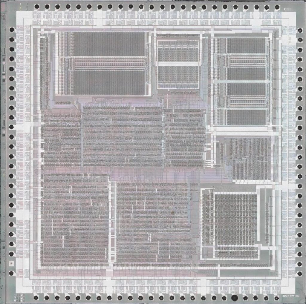
The final approach I can think of would be for us to acquire high-resolution die scans of the two SNES PPU chips, and then formally recreate transistor-perfect copies of them in a Verilog / VHDL-like language.
This would reveal to us all of the internal latches, and truly perfect emulation would now be possible: directly on FPGA emulators, and very rapidly in software emulators as well.
We currently have 20x decapped die scans of the PPU chips, courtesy of John McMaster, but we would need at least a 50x die scan (and preferably 100x) in order to trace out its logic.
The problem is, aside from the deeply flawed analog RGB method (which I simply don’t have the time for), I can’t really do this. And I don’t see anyone else working in open source emulation that is willing to do this either.
If you can help, please get in contact with me. If we can solve this last problem, we can have almost completely perfect SNES emulation, to a state where even I could be satisfied that the SNES has been preserved for future generations.
If you can’t help, I still appreciate you reading this, and hopefully it’s now more clear the final problems we have with SNES emulation, and why it’s so difficult to solve.
Thank you for reading!